(THEORY)
(DESIGN)
(ASSEMBLY)
(OPERATION)
(ATTENUATOR)
(HOME)
DDS RF Signal Generator
Matjaz Vidmar, S53MV
4. Operation
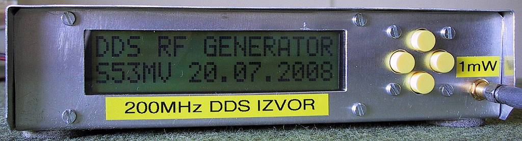
Immediately after power-up, the generator displays the software version/date for about one second:
About one second after power-up the display content is replaced by the mode and frequency in the top row and some more parameters in the bottom row. A blinking cursor shows the digit controlled by the UP and DOWN keys. LEFT and RIGTH keys select the digit. If there is no blinking cursor, then the UP and DOWN keys select the operating mode.
The frequency can be adjusted in 10Hz steps from zero up to 999.99999MHz. The software makes no reference to the actual DDS clock frequency at this stage. Therefore the frequency display just means that there will be some spectral component at the indicated value, but it does not tell whether it is the fundamental DDS product or a higher-order image.
In the CW mode the generator produces an unmodulated carrier. Besides the carrier frequency its relative amplitude can be adjusted from zero up to 200.0% of the nominal output level as shown on the following picture:

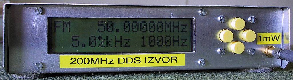
In the FM mode the generator produces a signal that is frequency modulated by an audio sinewave. The RF-signal level is set to the reference level (about 1mW at low frequencies). The peak deviation can be adjusted from zero to 999.9kHz and the audio modulation frequency can be adjusted from zero to 9999Hz in 1Hz steps as shown on the following picture:
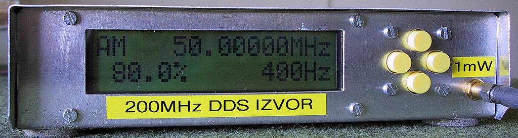
In the AM mode the generator produces a signal that is amplitude modulated by an audio sinewave. The carrier level is set to the reference level (about 1mW at low frequencies). The amplitude modulation depth can be adjusted from zero to 100.0% and the audio modulation frequency can be adjusted from zero to 9999Hz in 1Hz steps as shown on the following picture:
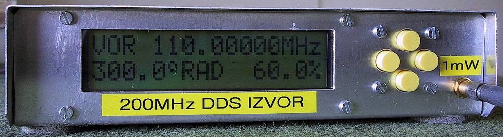
In the VOR mode the generator produces a signal that is amplitude modulated by a standard VOR aviation-beacon signal. The latter includes the 30Hz bearing signal and the 9960Hz audio subcarrier that is frequency modulated by the 30Hz reference with a deviation of +/-480Hz. The carrier level is set to the reference level (about 1mW at low frequencies). The VOR radial (phase difference between 30Hz bearing and reference) can be adjusted from zero to 359.9 degrees and the amplitude modulation depth (sum of 30Hz+9960Hz) can be adjusted from zero to 100.0% as shown on the following picture:
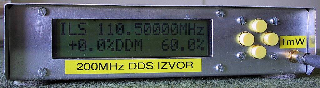
In the ILS mode the generator produces a signal that is amplitude modulated by a standard ILS (localizer or glideslope) aviation-beacon signal. The latter includes 90Hz and 150Hz sinewaves. The carrier level is set to the reference level (about 1mW at low frequencies). The ILS difference in depth of modulation (DDM) between the 90Hz and the 150Hz sinewaves can be adjusted from zero to the sum of both modulation depths and the latter can be adjusted from zero to 99.9% as shown on the following picture:
In the REF mode the DDS clock frequency can be adjusted while the generator operates in the CW mode. This allows a frequency counter or receiver to remain connected to the output and measure the frequency actually generated by the DDS. The CW level and frequency are shown in the bottom row but can not be adjusted in this menu:

Without any filtering of the RF DDS output, a conventional frequency counter will only show the correct frequency of the lowest (fundamental) spectral line of the DDS when the latter is less than about one third of the DDS clock frequency (less than about 65MHz) in CW mode. In other modes the modulation may interfere with the operation of the counter and this limit may be much lower.
All operating parameters of the DDS RF signal generator can be conveniently stored permanently into the EEPROM inside the LPC2138 microcontroller. There is just a single command to write the parameters into the EEPROM by depressing both LEFT and RIGHT pushbuttons simultaneously. The new parameters are written into the EEPROM only if a difference is found between the actual and stored parameters. In the latter case the display indicates the successful update of the EEPROM for about one second:

All parameters are copied from EEPROM to RAM at power-up RESET. When the DDS RF signal generator is powered up for the first time, the values of all parameters are meaningless and correspond to empty EEPROM locations. Therefore the first operation is to set all parameters in all different menus and most important the DDS clock frequency in the REF menu to some meaningful values and store them in the EEPROM.
The typical output spectrum of the DDS RF signal generator set to 35MHz is shown on the following picture (spectrum analyzer set to 50MHz/div horizontal resolution and 10dB/div vertical resolution):
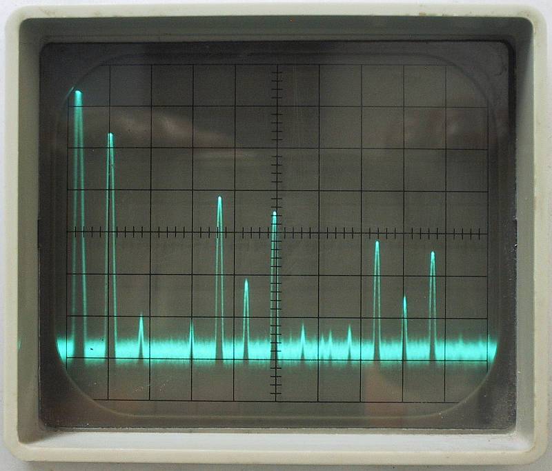
The highest peak on the left is the DC component, followed by the fundamental DDS signal at 35MHz. Many higher-order images are also visible. The image at 435MHz is less than 30dB below the fundamental signal, therefore this signal generator can be used for testing receivers in the 70cm band and even beyond. Clock crosstalk from the DDS chip at 200MHz and 400MHz is also well visible. The smallest peaks are produced by second-order nonlinearities elsewhere in the analog circuits.
Of course, the same output spectrum is obtained if the signal generator is tuned to 35MHz, 165MHz, 235MHz, 365MHz, 435MHz, 565MHz, 635MHz, 765MHz, 835MHz or 965MHz at a nominal DDS clock frequency of 200MHz. In the case of a different DDS clock frequency, the software makes all necessary computations so that there appears a spectral line at the desired frequency. One just has to keep in mind that there are many more lines elsewhere in the output-signal spectrum. Further, any signals close to the DDS clock or its harmonics are rather weak due to the sin(x)/x nulls.
When measuring the sensitivity of receivers and transceivers, it makes sense to keep a fixed 20dB SMA attenuator directly on the output connector at all times. This attenuator both reduces further shielding requirements and protects the DDS chip in the case of an unwanted transmitter activation. In any case it is recommended to use double-braid cables like the RG-223 or its teflon equivalents for all connections to and from attenuators while measuring receivers.
Additional menus could be developed to generate DTMF, CTCSS or other common signaling tones. A major limitation is represented by the DDS serial programming. The latter takes about 5 microseconds either by using the SPI1 interface or by direct software implementation in the LPC2138. Therefore the DSP interrupt rate can not be much higher than 100kHz in FM mode.
Recent DDS chips operate at clock frequencies up to 1GHz with much improved 14bit DACs on their outputs, producing cleaner output signals. All these chips have a similar serial interface to the CPU. Therefore the same LPC2138 microcontroller module could be used to drive new DDS chips, unfortunately including the speed limitations in FM mode.
Full-scale drawings, PDF datasheets, PCB files & ARM software

(THEORY) (DESIGN) (ASSEMBLY) (OPERATION) (ATTENUATOR) (HOME)